Saturday, October 8, 2011

5.5HP Turbo Charged Fuel Injected Engine

For a while now, I've been thinking about some of the shortcomings of my original fuel injection project.  I wanted to go back and redesign this project adding some of the missing pieces.  So, that said, the idea was to take a small carbureted engine and convert it to fuel injection, then add a turbo charger.  All of this would be controlled with a stand-alone ECU, and PC software to tune the parameters.

The Engine

There were a couple of options when it came to selecting the engine.  The main criteria was to select an engine that was small enough to bench test.  Although a larger engine would have helped when the turbo was installed (more displacement, would be able to reach higher boost) this one was good enough to prove out the concept.  It's a 4 cycle, 5.5hp engine with a horizontal output shaft.  It is similar to ones that you would find on a go-kart (GX160).

Controlling the Spark

These engines are equipped with a transistorized magneto, and the ignition is fixed at around 25 degrees BTDC (before top dead center).  Being able to set the spark advance gives you more control over the engine.  This is especially true if you can vary it according to engine load and RPM.  So the first step is to get some sensors mounted to engine to report on the cam shaft position, and when the engine has reached TDC.


Normally, we could use Hall-Effect sensors mounted near the teeth of the cam gear.  In this case, there wasn't an easy place to do this (at least I couldn't find one).  So instead, I chose to use a shaft encoder (CAM Position) and a break-beam IR Tx/Rx pair (TDC).  Future engines (yes, I plan on doing this again) will instead have the traditional Hall-Effect sensors mounted.

Next, the spark coil was added replace the magneto in order to fire the spark plug.  The initial test runs didn't have any special logic, the spark advance was adjusted manually from 15 to 31 degrees, just to see how the engine would respond.


Fuel Injection

The next step was pretty big.  It was going to involve removing the carburetor and adding a fuel injection system.  They don't typically make any parts for an engine this small, so a lot of time was spent trying to find parts that were small enough to retrofit onto the engine.

To supply fuel to the injector, an in-tank fuel pump was added (from a WRX).  It pressurizes the fuel line to 40psi, and the adjustable regulator maintains this pressure.  The original fuel injector was replaced with one from a Ford Festiva in order to reduce the flow rate (from 330cc to 120cc).


The throttle body is from an BMW R850 motorcycle which was restricted down to about 3/4" to better match the engine's intake.


Turbo Charger

Next was to add the turbo charger.  Actually, next was to find a turbo charger that was small enough for the engine.  The smallest available one I could find was a RHB31 (I'm told this is one from a Suzuki Swift 1.0l).  It would only be able to boost the engine between 2-4psi, but that would be enough for bench testing, so on it goes.


Since there engine does not have an oil pump, an evac pump is used to draw oil from the bottom of the engine through the turbo.  This keeps a vacuum in oil cavity preventing the oil from getting past the seals.  Normally an evac pump is used to pump excess oil away from the turbo when it's mounting point is low with respect to the oil pan.  This is typically not required if a turbo is mounted higher on the engine.

Drive by Wire Throttle

The last mechanical part that was added was a stepper motor mounted to the throttle body that controlled the throttle plate angle with a belt and pulley system.

Sensors

Along with the TDC and CAM position sensors, the engine is equipped with a MAP sensor, two temperature sensors (block temp, and intake air temp) and a TPS (throttle position sensor).  All of the sensor signals are routed back to the ECU board.  


ECU

The ECU is used to set the spark advance and fuel delivery based on the input sensor readings.  There are two main tables (Spark Advance and Fuel Delivery) that are user tunable using the PC software mentioned below.  The table values are set as a function of RPM and engine load, but correction factors for throttle input and temperature readings are also performed.


PC Software

In order to tune the engine, a PC application was developed to set the table values.  The application also reads back, reports and logs the sensor values to see how the engine is performing during the test run.  This allows you to see how the engine performs under different conditions and makes the tuning process much easier.


Completed Engine

A couple of pictures of the completed engine.

Quick Bench Test


June 13th, 2009

Video Capture Board

I started working on this project because I wanted to experiment a bit more with video (capture, display and scaling). I wanted to make the board flexible enough to experiment with a variety of input modes. To accomplish this, I placed a DVI header that accepts all of the common signals associated with DVI input chips (i.e. Data Lines, Control Lines, I2C for programming, etc.). Most of the available DTV decoder chips follow this format. The first board I will be experimenting with has both analog (YPbPr, VGA) and digital (HDMI) inputs. This allows me to attach several different types of inputs to the board. The output is basically a header of GPIOs. For now, I have a small 640x480p Sharp colour LCD.

The board is also equipped with USB so I can download data from the frame buffer. This will be useful when debugging, but can also be used to capture and dump frames.

Here is a screen capture of the current board. Only thing left to do is add a few control lines for the LCD.


September 8th 2007


1080p LCD Driver Board

This board was designed to demonstrate my current employer's DTV chip at CES in January of 2006.  It's purpose was to convert a DVI signal to LVDS and act as a stand-a-lone raw panel controller that would supply the data and control signals to power on the LCD and backlight. The panel used was a Samsung 46" 1080p (60Hz 8bit). It would accept DVI input and would output LVDS in the format required by the panel.

Most LVDS drivers support up to a 95MHz input clock (some newer ones up to 105MHz). The input data is then serialized and is output at a rate of 7x the clock. This means that for every input clock, 7 bits of data would be transmitted per channel.

Diagram of LVDS Driver Outputs for 8-bit JETDA Colour Format


Since there is a restriction on how fast the drivers can be clocked, achieving 148.5MHz (1080p, 60Hz, 8-bit) can be done be separating the odd and even pixels and sending the data separately using two drivers. Each driver would then effectively be transmitting at half the rate, or 74.25MHz.

The board consisted on a Silicon Image HDMI Receiver, two Thine LVDS transmitters, and an Atmel AVR microcontroller. The Silicon Image chip would convert decode the data and pass it along to the two Thine LVDS transmitters. The microcontroller was used to setup the turn-on sequence for the panel, and to program features in the Silicon Image chip using I2C. This board (and code for the microcontroller) was designed and assembled in four days in order to meet the trade show deadline.

Picture of the 1080p Raw Panel Driver Board


Pictures of the native 1080p panel being driven by the board


September 6th, 2007

PCI Bus Interface Card

The goal of this project is to create a PCI I/O target card along with a custom Windows driver.  The I/O card will use a Xilinx FPGA to connect to implement the PCI bus logic, and will communicate with a microcontroller via an 8-bit bidirectional bus.  The microcontroller will be used as an intermediatedevice to interconnect other peripherals such as A/D converters and real time clocks.

A master or initiator is an agent that initiates transactions on the PCI bus. The master controls data transfer to and from the target. To initiate a data transfer, the master must assert the required signals, and keep them asserted until they are acknowledged. A target or slave is an agent that responds to a transaction initiated on the PCI bus (by a master agent) and intended for it. To indicate completion of a transaction, a target must provide an acknowledge cycle, which can include error or retry signals. The PCI interface automatically inserts any wait states needed to prevent the master from timing out, allowing high-speed PCI transactions to be processed by relatively slow back-end devices.

A PCI back-end device is defined as any device that stores, sends, or retrieves information using the PCI bus (for example: video cards, memory cards, disk drives, and multimedia cards). In a conventional configuration, the back-end device is considered a target. The target interface logic and memory can either is encapsulated in a controller device or fully or partially integrated into the back-end device.

The back-end device is physically remote from the processor local bus. Back-end devices communicate with the host processor across a PCI bridge, which serves as a layer of device management between back-end devices and the host, thereby streamlining data transfer. The interface supports bus mastering, which allows intelligent devices to access main memory directly.


In order to understand the operation of the PCI module that was tested, it is necessary to present and explain each of the signals that will be used on this device. As specified in the PCI Bus Specification, many of these signals are active low, which means that it is asserted at low voltage. We will distinguish this type of signal from the others using an 'n' in front of any signal that is active low. These definitions are taken from the PCI Local Bus Specifications (2.2), as the expected behavior of the signals on a PCI device.

The signals used by this device can be divided into different groups. These types are the following:

in - Input is a standard input-only signal.
out - Totem Pole Output is a standard active driver.
t/s - Tri-State is a bi-directional, tri-state input/output pin.
s/t/s - Sustained Tri-State is an active low tri-state signal owned and driven by one and only one agent at a time.

PCI pin functions can vary depending on the purpose of the device. In other words the behavior of a pin in a PCI device that is a target is not necessary the same as if it were a master. Since our interest is only on a PCI device that will perform as a target, we will only present the functions of the pins in a target. The block diagram below shows the signals used on a target PCI device.

Block diagram of a PCI device showing Required and Optional Signals.


The PCI pin definitions will be organized by functional group. The first of the functional are the System Pins; these are signals that come from the system in which the device in mounted. Most of the time a processor regulates these signals.

System pins on the PCI Target device.


Name
Type
Behavior
Description
CLK
in
in
Clock provides timing for all transactions on PCI and is an input to everyPCI device. All other PCI signals, except nRST, are sampled on the rising edge of CLK and all other timing parameters are defined with respect to this edge. PCI operates up to 33 MHz.
nRST
in
in
Reset is used to bring PCI-specific registers, sequencers, and signals to a consistent state. Anytime nRST is asserted all PCI output signals must be driven to their benign state. In general, this means they must be asynchronously tri-stated. nRST may be asynchronous to CLK when asserted or deasserted. Although asynchronous, deassertion is guaranteed to be a clean, bounce-free edge. Except for configuration accesses, only devices that are required to boot the system will respond after reset.


The second functional group is the Address and Data Pins. The signals on these pins are the ones that carry the commands and address of the data that should be transferred through the device.

Address and Data pins on the PCI Target device.


Name
Type
Behavior
Description
AD[31::0]
t/s
Bi-dir.
Address and Data are multiplexed on the same PCI pins. A bus transaction consists of an address 3 phase followed by one or more data phases. PCI supports both read and write bursts. The address phase is the clock cycle in which nFRAME is asserted. During the address phase AD[31::00] contain a physical address (32 bits). For I/O, this is a byte address; for configuration and memory, it is a DWORD address. During data phases AD[07::00] contain the least significant byte(lsb) and AD[31::24] contain the most significant byte (msb). Write data is stable and valid when nIRDY is asserted and read data is stable and valid when nTRDY is asserted. Data is transferred during those clocks where both nIRDY and nTRDY are asserted.
nC/BE[3::0]
t/s
in
Bus Command and Byte Enables are multiplexed on the same PCI pins. During the address phase of a transaction, nC/BE[3::0] define the bus command. During the data phase nC/BE[3::0] are used as Byte Enables. The Byte Enables are valid for the entire data phase and determine which byte lanes carry meaningful data. nC/BE[0] applies to byte 0 (lsb) and nC/BE[3] applies to byte 3 (msb).


The Interface Control Pins are the signals that come from the PCI Bus and determine if the transaction start, stop, or end in combination with each other and with other signals.

Interface Control pins on the PCI Target device.


Name
Type
Behavior
Description
nFRAME
s/t/s
in.
Cycle Frame is driven by the current master to indicate the beginning and duration of an access. nFRAME is asserted to indicate a bus transaction is beginning. While nFRAME is asserted, data transfers continue. When nFRAME is deasserted, the transaction is in the final data phase or has completed.
nIRDY
s/t/s
in.
Initiator Ready indicates the initiating agent's ability to complete the current data phase of the transaction. IRDY# is used in conjunction with TRDY#. A data phase is completed on any clock both IRDY# and TRDY# are sampled asserted. During a write, IRDY# indicates that valid data is present on AD[31::00]. Wait cycles are inserted until both IRDY# and TRDY# are asserted together.
nTRDY
s/t/s
Bi-dir.
Target Ready indicates the target agent's ability to complete the current data phase of the transaction. nTRDY is used in conjunction with nIRDY. A data phase is completed on any clock both nTRDY and nIRDY are sampled asserted. During a read, nTRDY indicates that valid data is present on AD[31::00]. During a write, it indicates the target is prepared to accept data. Wait cycles are inserted until both nIRDY and nTRDY are asserted together.
nSTOP
s/t/s
Bi-dir
Stop indicates the current target is requesting the master to stop the current transaction.
nDEVESEL
s/t/s
Bi-dir
Device Select, when actively driven, indicates the driving device has decoded its address as the target of the current access. As an input, nDEVSEL indicates whether any device on the bus has been selected.
IDSEL
in
in
Initialization Device Select is used as a chip select during configuration read and writes transactions.

Bus Commands

Bus commands indicate to the target the type of transaction the master is requesting. Bus commands are encoded on the nC/BE[3::0] lines during the address phase.

Commands for the PCI device


nC_BE[3::0]
Command Type
0000
Interrupt acknowledge
0001
Special cycle
0010
I/O read
0011
I/O write
0100
Reserved
0101
Reserved
0110
Memory read
0111
Memory write
1000
Reserved
1001
Reserved
1010
Configuration read
1011
Configuration write
1100
Memory read multiple
1101
Dual address cycle
1110
Memory read line
1111
Memory write and invalidate


PCI Characteristics

The PCI bus has 4 main characteristics:
  • Synchronous
  • Transaction/Burst oriented
  • Bus mastering
  • Plug-and-play

PCI is Synchronous

The PCI bus uses one clock. The clock runs at 33MHz by default but can run at higher rates if your hardware supports it.

The PCI bus is transaction oriented.

1. A transaction is started

2. A starting address is specified (one clock cycle)

3. One or many data cycles follow

4. The transaction is ended.

Once the address is specified, many data cycles can follow without the need to retransmit address information.  The address is auto-incremented at each data cycle. To specify a different address, the transaction would have to be stopped, and a new one started. For this reason, PCI bandwidth is best utilized in burst mode.

PCI Bus Mastering

PCI transactions work in a master-slave relationship. A master is an agent that initiates a transaction (can be a read or a write).
While the host CPU is often the bus master, all PCI boards can potentially claim the bus and become a bus master.
 
PCI is PnP (Plug-and-Play)

The last feature is an important part of plug-and-play. Each board responds to some addresses, but the addresses to which it responds can be programmed (i.e. each board generates its own board/chip-select signal(s)). This allows the OS to "map" the address space of each board appropriately.

PCI Memory Spaces

PCI defines 3 memory spaces where you can read and write data.
When a transaction starts, the master specifies the starting address of the transaction, if it's a read or a write, AND which space he wants to speak to.

1. Memory space
2. IO space
3. Configuration space


They work as follow:

  • The memory and IO spaces are the workhorse spaces. They are "relocatable" (i.e. the addresses at which each board responds can be moved).

  • The configuration space is used for PnP. It's a space where each board has to implement very specific registers at very specific addresses, so that the host-CPU/OS can figure out what is each board's identity/abilities/requirements. The host CPU/OS can also write to enable and configureboards other two spaces.

  • This space is fixed and always starts at address 0 for all PCI boards; so one line of the PCI connector is used as board-select (for this space only).

To be compliant, a PCI board needs to implement configuration space. Memory and IO spaces are optional, but one or both are always used in practice.

PCI Voltage

PCI boards currently use 3.3V or 5V signaling. The connectors and correspondingly the boards, are "keyed" to identify whether it is 3.3V or 5V compliant. This is to ensure that a 3.3V only board cannot be plugged into a 5V-only bus.
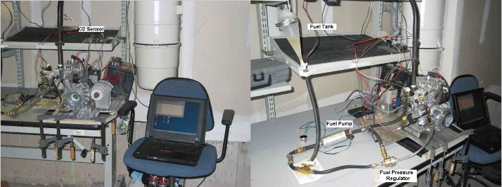
PCI Prototype Card

Here is a snapshot of the work-in-progress Target PCI Card with a brief description of the populated components:

Xilinx Spartan II FPGA (XC2S100) TQFP144

XC1801SO20 Configuration PROM

FTDI FT245M USB Interface Chip

TPS7225 2.5V Fixed Voltage Regulator (Xilinx Core Voltage Supply)

5V 32-Bit PCI Card Interface


The Xilinx Spartan II was selected based on several factors. First, Xilinx offers a free downloadable Webpack for this family, and the JTAG programmer is straight forward to construct. This allows me to spend little time (and money) to setup and get started with the tools. Also, the Webpack is not time limited, or constrained in any way that would prevent me from taking advantage of all the features available on the FPGA. Secondly, although the available core voltages for this device are 1.8V and 2.5V, it still maintains 5V PCI-Bus compatibility on the I/O ring. This is important since most of the test PCs I'm willing to risk during the prototyping stage all operate on a 5V PCI Bus.

I have also added a USB interface chip to this card for future debugging operations or to integrate external add-on devices.

Currently the card is capable of responding to I/O and Memory space reads and writes. The initial tests used a fixed address to generate hits in both the I/O and Memory areas. I have just completed the implementation of the configuration space write operation (specific registers only) to allow for OS PnP (plug and play). This will allow the OS to give the PCI Target Card a valid I/O and Memory space address automatically.

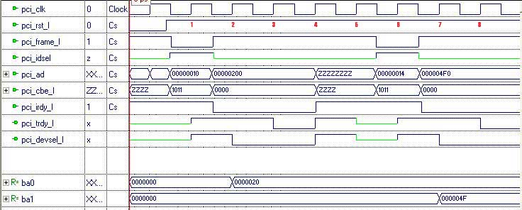
Here is a screenshot of the configuration simulation performed in ALDEC Active-HDL. This screenshot shows two PnP addresses being written to the internal PCI Target Card registers ba0 and ba1 respectively.


Description of Events

PC asserted the nFRAME signal on rce (rising clock edge) 1 indicating the start of a transaction. At the same time, it places the configuration address of 10h (Base Address 0) on the AD lines and sets nCBE to 1011 (Configuration Write). Also, the IDSEL line is asserted indicating that this specific device has been selected. The IDSEL line is unique to each PCI bus slot, and is used at start-up to configure each card with appropriate addresses.

By rce 2, the PC has asserted the nIRDY, indicating that the data is ready to be written (200h). The PCI Target card asserts the nDEVSEL indicating that it has acknowledged the fact that it has been selected. This is also the time when the base address register 0 (ba0) records the PnP address.

Since by rce 3 the nTRDY signal has not yet been asserted, the PC will continue to hold the nIRDY signal low.

By rce 4, the transaction has completed, and the bus returns to the idle state.

This operation is repeated again to write the second PnP base address to ba1.

October 3rd, 2004

I2C Snooper Board

While working at my current employer, my group had a need for an I2C bus monitor. There are quite a few devices that we use on a daily basis that communicate with the I2C bus protocol, so having a monitoring tool would be useful.  After searching the web for products, it became apparent that if you wanted a monitor that would be able to snoop at both standard (100kHz) and fast (400kHz) modes without being intrusive to the bus, you would need to spend a bit of money. 

An example of this would be one from Equinox http://www.equinox-tech.com/products/details.asp?ID=336 that sells for $4000.  Some of the other models we looked at were less expensive but could not capture data at 400kHz, or would stall the bus by pulling the clock line low in order to keep up with the data transfer.  So, why not custom build one that would cost a fraction of the cost with the same functionality, and be able to customize it further when needed.

Capture Board
Initially, I designed a board that would communicate over the serial port and not require any additional drivers.  The user interface was implemented in the microcontroller and had a DOS-like feel to it.  Below are a few screen captures of the first cut:

I2C Bus Capture Firmware Running on the ATMega128 (Help Screen)


Reading and Writing Data to EEPROMs


Data Capture in I2C Standard Mode (100kHz)


This was fine, but there were one shortfall that was known before proceeding.  If you wanted to capture data at bus speeds above 100kHz, you would need to buffer the data since the serial port would not be able to handle the data stream in real-time.  The problem with buffering the data is if you are recording over a long period of time, with heavy bus traffic, you will eventually run out of buffer space.  Since this was most likely the type of scenario we would encounter, an alternative approach was needed.  So, to make a long story short, I decided to add a USB chip to the device to up the speed.

I2C Snooper Take Deux

I wanted to keep the basic functionality the same (meaning, ability to read/write and capture data) but be able to do it at 400kHz.  So, I started by adding a USB 1.1 chip by FTDI, the FT245BM.  This chip would allow me to communicate at speeds up around 1MB per second, so sending I2C bus data with some overhead even at 400kHz would not be a problem.  Since the FTDI chip was so fast, I found that I didn't need any external SRAM to pre-buffer the data, the 384 byte internal buffer was good enough.  This also meant that I wouldn't need to use the ATMega128 with external SRAM capability, so it was replaced with an ATMega32.  Actually, I could have brought the cost down further by using an ATMega8, but I wanted to have some extra internal SRAM and Flash just in case extra functionality was needed.

Here is a screen capture of the board file:


 a picture of the populated board:


The MFC Application

After the board layout was complete, I needed to write a application to interface with the board.  Initially I wanted to avoid doing this, but since I needed to add a USB driver chip, I didn't have a choice.  The software was written in VC 6.0 (using MFC) as a multithreaded application.

There are two threads which take care of the incoming data.  The first is used to strictly capture the data stream and place it directly into a thread-safe queue.  The second thread is used to remove data from the queue, parse it, and display the captured bytes to the screen.  The software framework is setup only for I2C data capture at the moment, but since the AVR controller has a built-in I2C peripheral, the software can be easily modified to act as an I2C Master or Slave device.  At the moment though, capturing data seems to be more important.  Here is a screen capture of the MFC application:

MFC Application Capturing data at 412kHz


What's left?  Well, I am currently working on triggering and filtering which will be completed in about a week.  This is rather easy to implement since all the data is available in the application.

The Cost

One of the main reasons for starting this project was to try and keep the price of the unit low.  Material costs for the board, including setup and shipping charges for the prototype boards totaled $160.  The price per board is about $25.

July 10, 2005

High Resolution CCD Scanner

In June, this project was entered in the 2004 AVR Design Contest sponsored by Atmel and Circuit Cellar.  It ended up winning a Distinctive Excellence Award based on technical merit and unique usage of an AVR microcontoller.


Many embedded systems today require several aspects of digital and analog electronics to create an end product. Depending on the application and product volume, specialized hardware such as  ASICs/CPLDs are used when high speed signal processing is required, especially when timing is critical to the performance product.

A good example of this would be a digital scanner. Scanners utilize a CCD element (either full or fractional width) that capture an image by exposing a pixels for a given time (Tint - Integration Time) which is converted to a voltage that represents black (or white) intensity.  When scanning a document in grey scale or colour, Tint becomes a critical parameter in obtaining uniformity and image quality.  Slight variations in grey/colour levels between pixels are easily visible by the human eye.
With that said, I thought that it would be interesting to see if I could design a scanner that would be able to reproduce photographic quality pictures using only scrapped parts.

CCD Sensor
I was able to salvage the image portion of an old photocopier. Unfortunately, the mechanism for moving the image scanner across the page was damaged, so all I was able to salvage was the CCD portion.

On older units like this one, a small CCD like this one is positioned behind a lens that reduces the actual width of the image to the size of the CCD viewing area (approx 3-4cm). In order to maintain the correct size, two or three mirrors are used to obtain the correct focal distance. To make things even more complicated, the focal distance is maintained across the page by moving the mirrors at different rates. So, needless to say, correcting the transport on my unit was not going to be an easy task.

On newer scanners and photocopiers, the CCD is stretched across the width of the page (1 to 1 ratio). This eliminates the need for mirrors and lenses, thereby making the optical design less complicated. However, in order to make the scanner portion cost effective, the CCD lens is usually integrated directly on the PCB, along with the other electronics needed for image capture. This makes isolating the CCD or finding a functional description more difficult.

So, I decided to use the small CCD at a 1 to 1 ratio. This allows me to get around the image focus problem, but now reduces my effective scanning width to 3.5cm. Oh well, if I ever find another unit, I could always connect the board to the CCD and obtain full size images. Until then, I will be able to take amazing scans of stamps :)
The CCD used in this photocopier is a TCD1502C. It is a linear image sensor with a single row of 5000 photodiode elements. It is capable of producing 400dpi across an A3 page (lens system), and each element is 7um x 7um x 7um. When I operate this CCD at a 1 to 1 ratio, the effective scanning resolution is:

5000 elements * 7um per element = 3.5cm of viewing area.

3.5cm / 2.54 cm per inch = 1.378 inches

5000 elements / 1.378 inches = 3628 elements per inch (or > 3600dpi). Good enough for stamps :)

In order to use the CCD at a 1 to 1 ratio, you will need to provide a way to straighten the incoming image onto the CCD. This is done by using a SELFOC™ lens. This lens is basically made up of optical light pipes that "straighten" the light before it reaches the CCD.


The lens is positioned above the CCD at a fixed distance determined by the properties of the lens.  The image (on the top side of the glass) must also be a predetermined distance away from the top of the lens in order to maintain focus. 

Here's where I put my machining skills to the test... Time to create a transport system for the scanning element.  Since the pixel dimensions are 7um x 7um, I will need to move the image transport 7um at a time in order to maintain the correct aspect ratio.  Using a lead screw linear table and a stepper motor, I am able to achieve this resolution.

Below is a picture of the completed scanner with some key components highlighted:


Stepper Motor Driver (Full and Half Step Mode)


Block Diagram


ALTERA MAX 7064
As I mentioned earlier, Tint  (Integration Time) is critical to uniformity and image quality since the exposure time of each element will determine the level of brightness it views. In order to properly control the exposure time, I used a MAX7064 to generate the timing for the CCD, as well as a built in address generator and multiplexer to store the A/D result to SRAM.

The principal of operation is as follows; the MAX chip will constantly scan the CCD, thus ensuring that Tint is maintained. The SRAM is shared between the microcontroller and the MAX chip, so it is the responsibility of the the microcontroller to signal when it has relinquished the bus, allowing the MAX chip to save the current line data directly to the SRAM.  The microcontroller waits for the MAX chip to signal completion, then transfers the data to the PC.

Image of the CCD Sensor timing waveform taken from a Logic Analyzer:


Scope Trace of Test Pattern (Analog Signal)

The test pattern consisted of three parallel vertical lines centered around 60 degree angled chevron lines.


Atmel AT90S8515 microcontroller
The microcontroller is responsible for synchronizing the scanning, advancement of the stepper motor and transfer of image data.  Control of the MAX chip is managed by a pair of signals which indicate when to begin scanning, and when scanning has completed.  The "START" signal (microcontroller -> MAX) indicates that the microcontroller has relinquished the SRAM bus and is waiting for MAX chip to write the current line data to SRAM.  Once this has completed, the MAX chip raises the "DONE" signal.  The microcontroller then begins to transfer the data out of SRAM to the PC.  The stepper motor then advances the CCD by one line, and the cycle repeats until the requested number of lines have been scanned.

PC Application (CCD Mini Scan)
The sole purpose of the PC application is to compile and view the scanned image (along with some other manual functions).  The application was written in LabWindows CVI v5.5.  Data transfer between the microcontroller and PC is performed serially using a PAR protocol.  To test the resolution of the scanner, I scanned the micro print found on the American $10 and $20 dollar bill, here are the results:
$10 - Above the name "Hamilton" reads "THE UNITED STATES OF AMERICA" and inside the "20" on the bottom left hand side reads "USA20".


The CCD scanner board is also capable of performing image adjustments in real time before passing the image data to the PC application.  Below is a sample of the possible image adjustments that can be made: 

Original Image (Actual Size):                    Magnified View of Original Image:
 22mm x 26mm

Scanned Image on PC Application Screen:
No image adjustment is preformed by the PC application, the application displays the raw data as sent from the scanner board.

                                              Normal                            Brightness High
                                          Brightness Low                          Contrast Low
                                          Contrast High                       Edge Enhancement
                                            Engrave                                    Negative
                                            Emboss                             Black and White
                                                                      Outline

After seeing the results, all of the work seemed well worth it.  This project covered aspects of: embedded programming, WindowsTM programming, protocol development, VHDL design, analog /digital electronics and finally mechanical design.

Scanning micro print on a US $10 dollar bill:


August 20th 2004

4-Stroke Engine Fuel Injection

A colleague of mine who was a co-op student at my one of my previous employers, was involved in his forth year design project.  He had mentioned to me how they were building a high mileage car based on a Briggs and Stratton™ 3hp motor.  The idea was to get the vehicle to travel the furthest distance on the least amount of fuel.

The current setup (as with any standard lawnmower engine) was based on a carbureted intake manifold.  Students from previous years already modified the engine with a CAM position sensor and had fitted the engine with a motorcycle intake.  The reason behind adding a fuel injection delivery system was that the engine could be tuned dynamically to run with less fuel (running the engine "leaner").  After his project was submitted (and final grades were determined), I decided to develop a tunable fuel injection system for this engine.

The sensors that were available were a TPS, O2 sensor, and TMPS.  A helpful addition would have been a MAP (manifold absolute pressure) sensor, however the intake manifold at the time was not modified to accommodate one.

Functional Descriptions of Sensors

TPS (Throttle Position Sensor): The throttle position sensor determines the open angle of the throttle plate.  This information is used to detect if the throttle plate is closed, wide open, partially open, and the rate of change of throttle position.  The sensor is basically a potentiometer with an overall resistance of 5,000 ohms, +/- 25%.

O2 (Oxygen) Sensor: The oxygen sensor monitors the level of oxygen (O2) in the exhaust so an onboard computer can regulate the air/fuel mixture. The sensor is mounted in the exhaust manifold and generates a voltage signal proportional to the amount of oxygen in the exhaust.  When the air/fuel mixture is rich and there is little O2 in the exhaust, the difference in oxygen levels across the sensing element generates a voltage through the sensor's platinum electrodes: typically 0.8 to 0.9 volts. When the air/fuel mixture is lean and there is more oxygen in the exhaust, the sensor's voltage drops to 0.1 to 0.3 volts. When the air/fuel mixture is perfectly balanced and combustion is cleanest, the sensor's output voltage is around 0.45 volts.

TMPS (Temperature Sensor): The temperature sensor is used to monitor the temperature of the air/fuel mixture in the intake manifold.  It uses this information, in addition to the manifold pressure, to calculate the density of the air entering the engine. 

MAP (Manifold Absolute Pressure) Sensor: (Would have been nice to have) The MAP sensor determines the absolute pressure (not the relative-to atmospheric pressure) of the air inside the intake manifold and the atmosphere (barometric pressure).

Here are a couple of close-up pictures of the motor and intake manifold.  In the picture on the left, you can see the fuel injector clearly.  The Temperature Sensor is not visible as it is located on the opposite side of the intake at the position marked "TMPS".  Also, the Throttle position sensor is on the opposite side of the throttle plate CAM (marked "TPS").


Here are a few more pictures of the complete setup.  In the picture below on the left, you can see the O2 sensor mounted on the exhaust pipe to the left of the position marked "O2 Sensor".  In the picture below on the right, you can see the fuel tank, fuel pump and  fuel pressure regulator.


There were several steps involved in setting up the fuel injection controller.  Let me summarize the steps below:

The throttle plate open angle was divided into 500 positions.  The first objective was to determine the base injector "on time" which was the minimum on-time required to keep the engine running while at idle.  This number was finalized once the engine had been running for a period of time long enough to warm up the O2 sensor to its operating temperature.

Next, each of the 500 throttle plate positions required tuning to the proper injector on-time (this was the most tedious part of the setup).  The injector on-time was tuned so that the O2 sensor would report a less than perfect air/fuel (lean) mixture (approx. 0.3V).  This became the "base" or "ideal" injector on-time for the engine.  The settings for each of these positions were stored in the EPROM of the micro controller.

Cold starts required more fuel to get the engine running.  After a few cold start attempts, the delta was determined and added to base injector on-time.  As the engine warmed up, so did the air entering the cylinder which resulted in less fuel needed for combustion.  The TMPS would be used to gradually reduce the delta to zero, bring the injector on-time back to the preset "base" timing.
The only trouble point that remained was when an abrupt change in the throttle position was encountered.  Since the engine was already running lean, quick changes in the throttle plate position (opening) would cause the engine to cut-out. The solution to this was to add another delta that would increase the injector on-time to prevent the engine from stalling.  Ideally, if you are trying to keep fuel consumption down, quick acceleration should be avoided. Once the throttle plate had stabilized, the controller would slowly return the engine to the default "base" timing.

The Fuel Injector controller was also equipped with a RS-232 port.  All of the settings including the fuel map, cold-start delta, throttle plate delta could be accessed, modified and stored using a lap-top computer.  This allowed the engine parameters to be "tweaked" if needed on the spot  without having to recompile and flash new software.  The port could also report the status and readings of each sensor to validate proper operation. 

Here are a few pictures of the Fuel Injection controller board:


May 23th, 2003